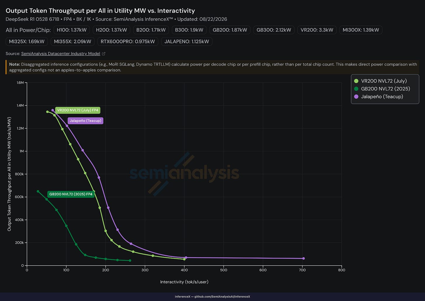
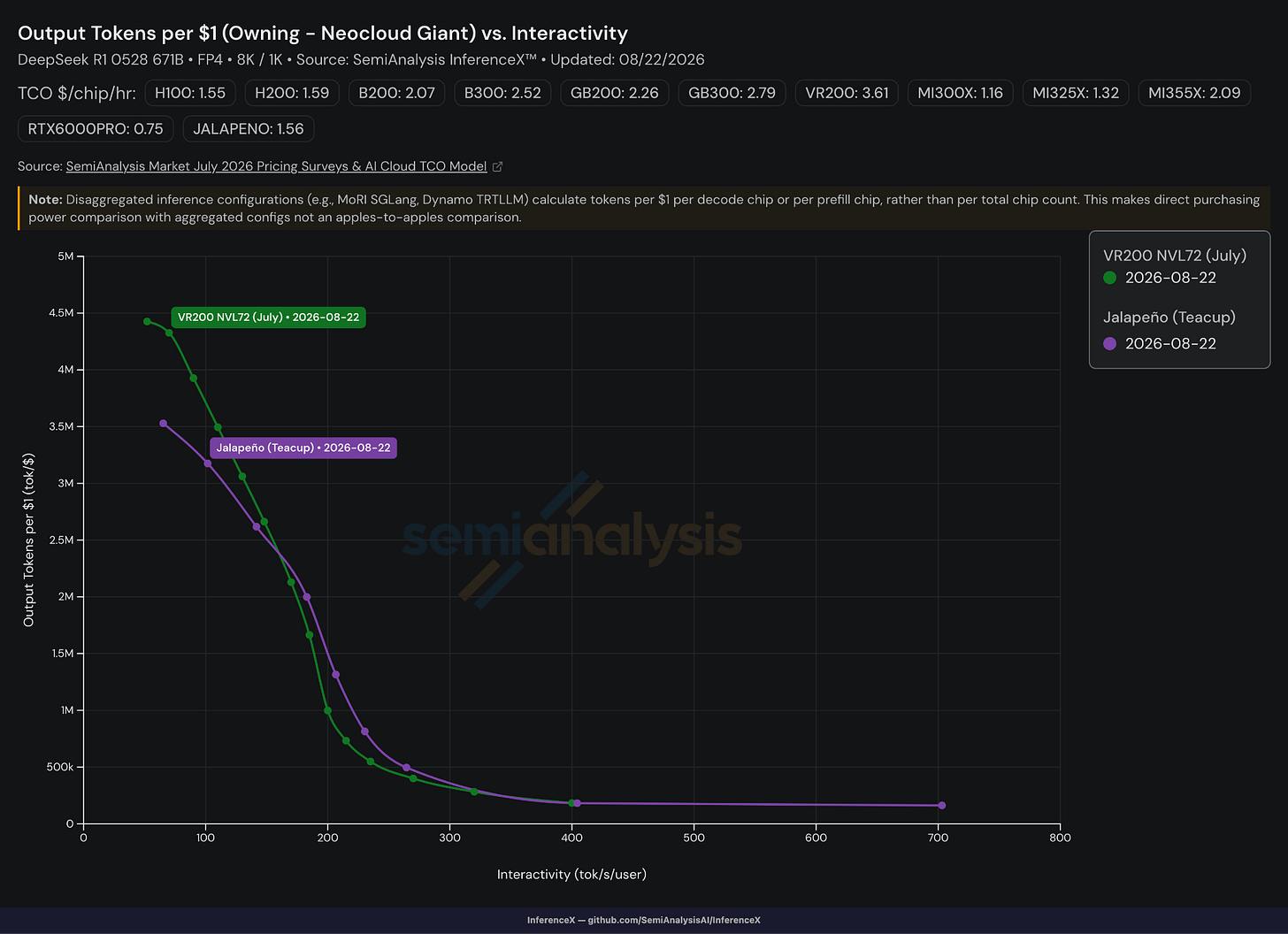
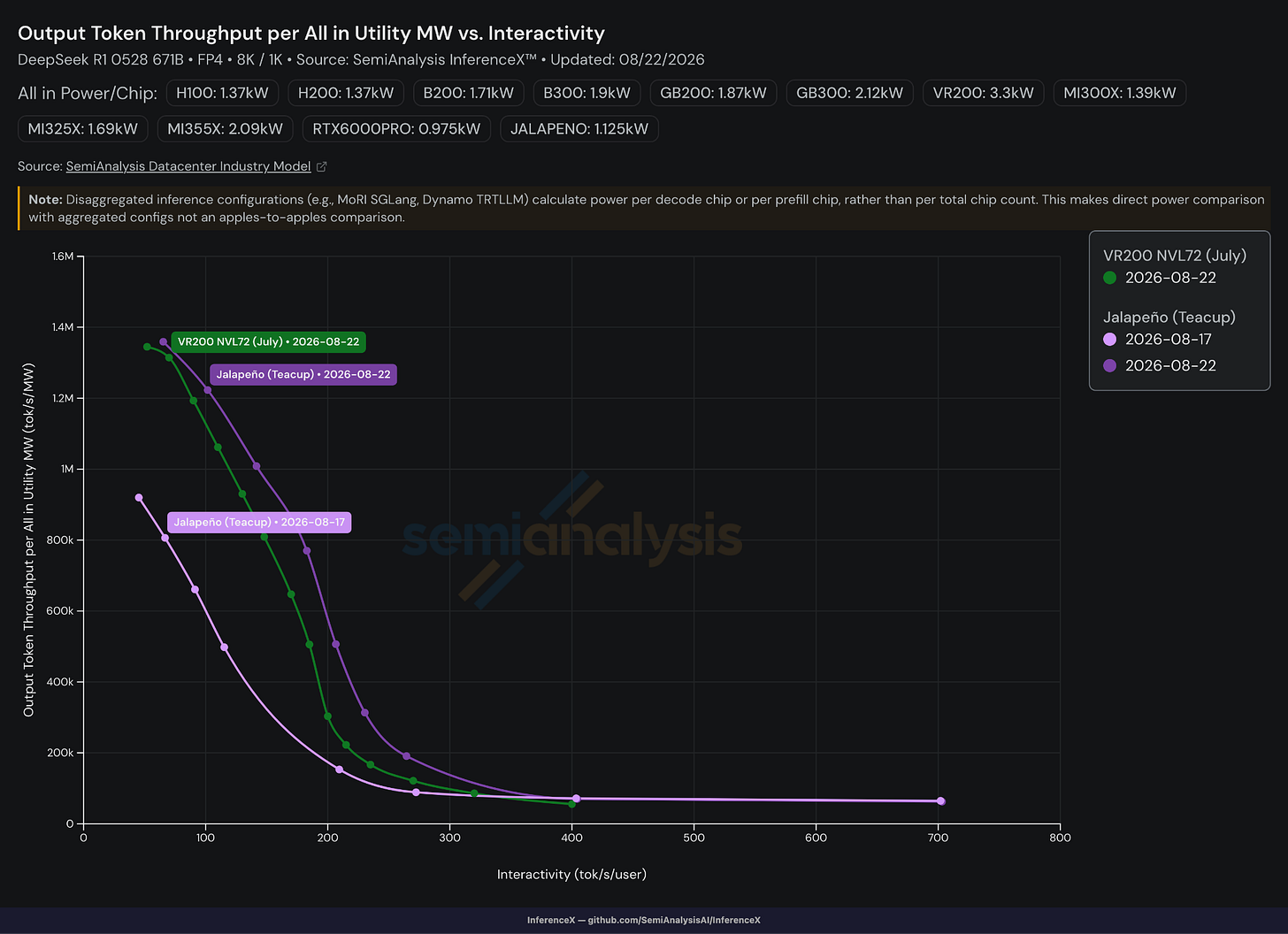
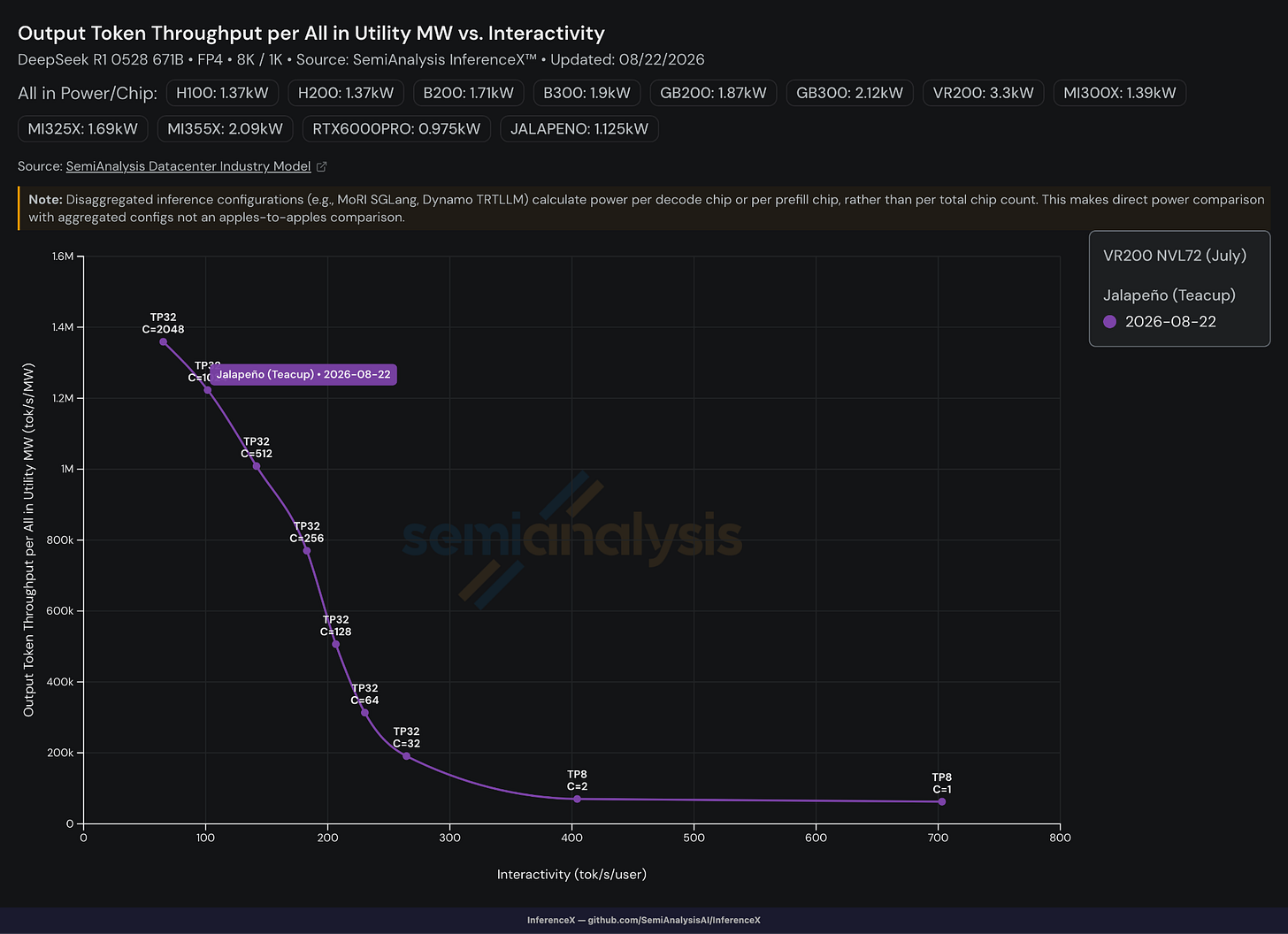
On perf/TCO, Vera Rubin and Jalapeño are head-to-head, producing almost the same number of output tokens per $. However, as previously mentioned, Jalapeño’s results are obtained without speculative decoding and Vera Rubin’s results use speculative decoding. Speculative decoding leads to a ~3-5x reduction in cost per token. When speculative decoding is implemented on Jalapeño, this will enable Jalapeño to serve tokens even more cost effectively. Of course, part of this TCO advantage comes from trading Nvidia’s high margins for Broadcom’s lower (though still high) margins. But this is not all of it. For example, Meta and Microsoft’s AI ASIC programs not getting off the ground despite being at it for much longer shows that cost is only one part of the equation. For Jalapeño’s full TCO breakdown, see the SemiAnalysis AI Cloud TCO model .
Source: OpenAI, SemiAnalysis
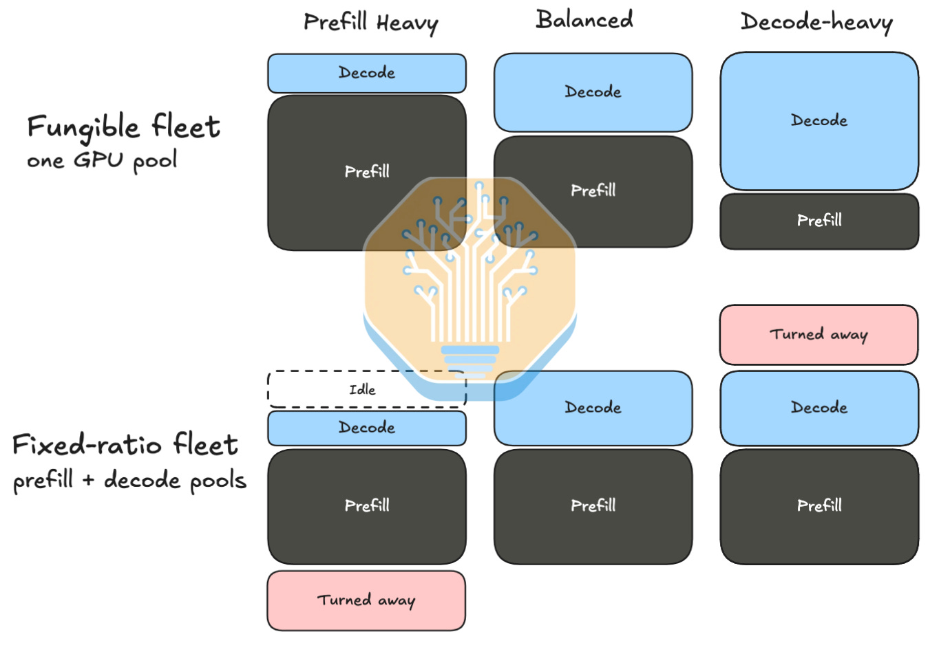
Architecturally, OpenAI chose not to disaggregate prefill and decode (PD) across separate chip pools. The draft model and main model share the same chips and fabric, a design philosophy that trades some theoretical efficiency for practical operations. The motivation is that the workload mix changes over time, for example the ratio of input to cache write to cache read to output tokens has changed significantly as we have moved through the three eras of models ( knowledge, reasoning, and agentic, as discussed in our recent article ). Therefore, picking a fixed amount of heterogenous prefill silicon and decode silicon up front can lead to inefficiencies over time. OpenAI chooses a homogenous pool in this architecture and tries to make the chip perform well on everything.
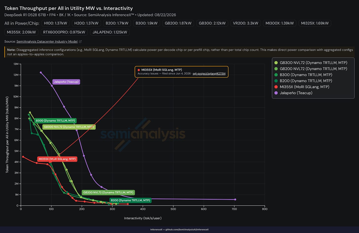
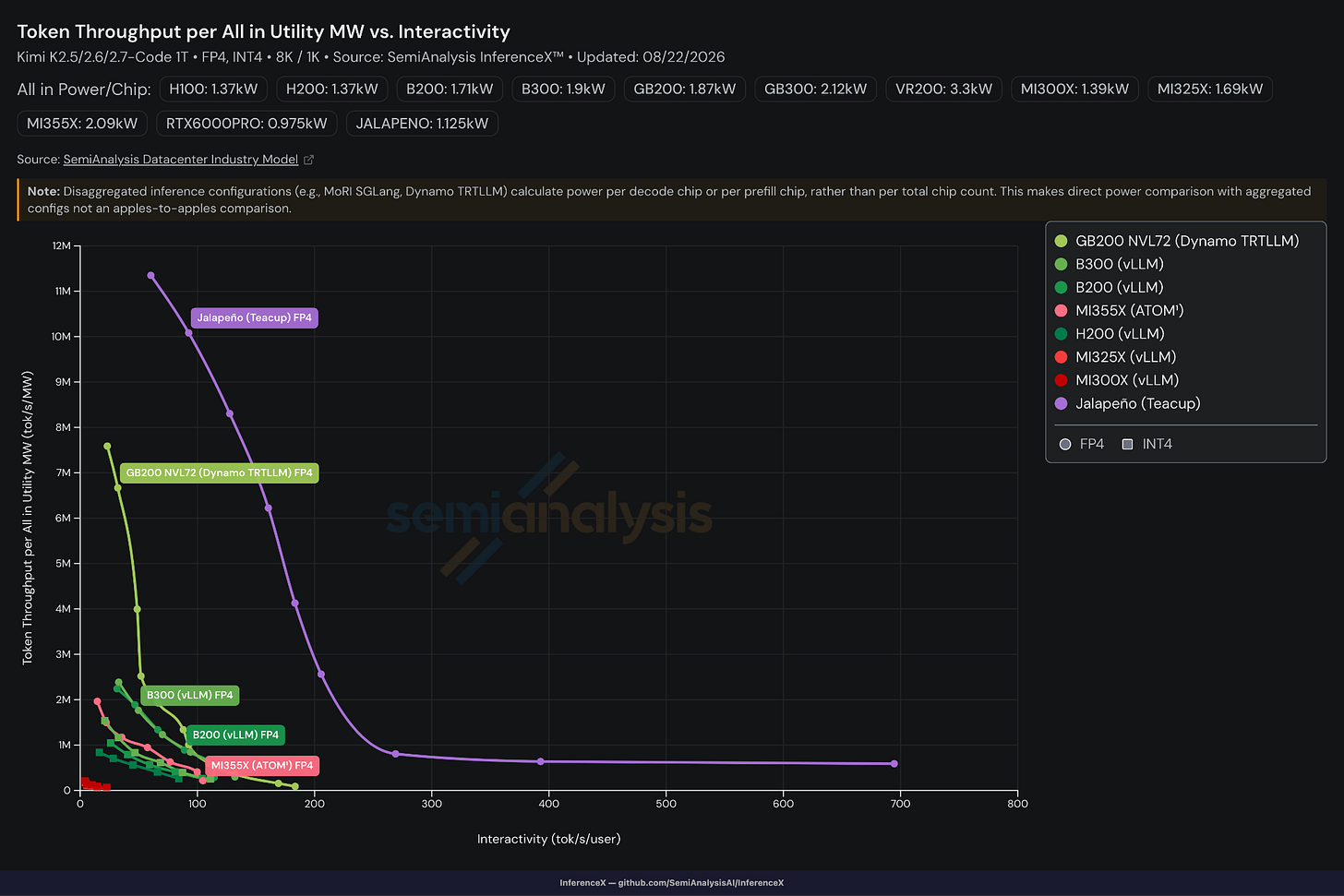
And it does. On Kimi K2.5 (which Cursor Composer 2.5 is based on), Jalapeño reaches nearly 700tok/s/user and more than 9x the next best performing chip at 100tok/s/user.
Source: OpenAI, SemiAnalysis
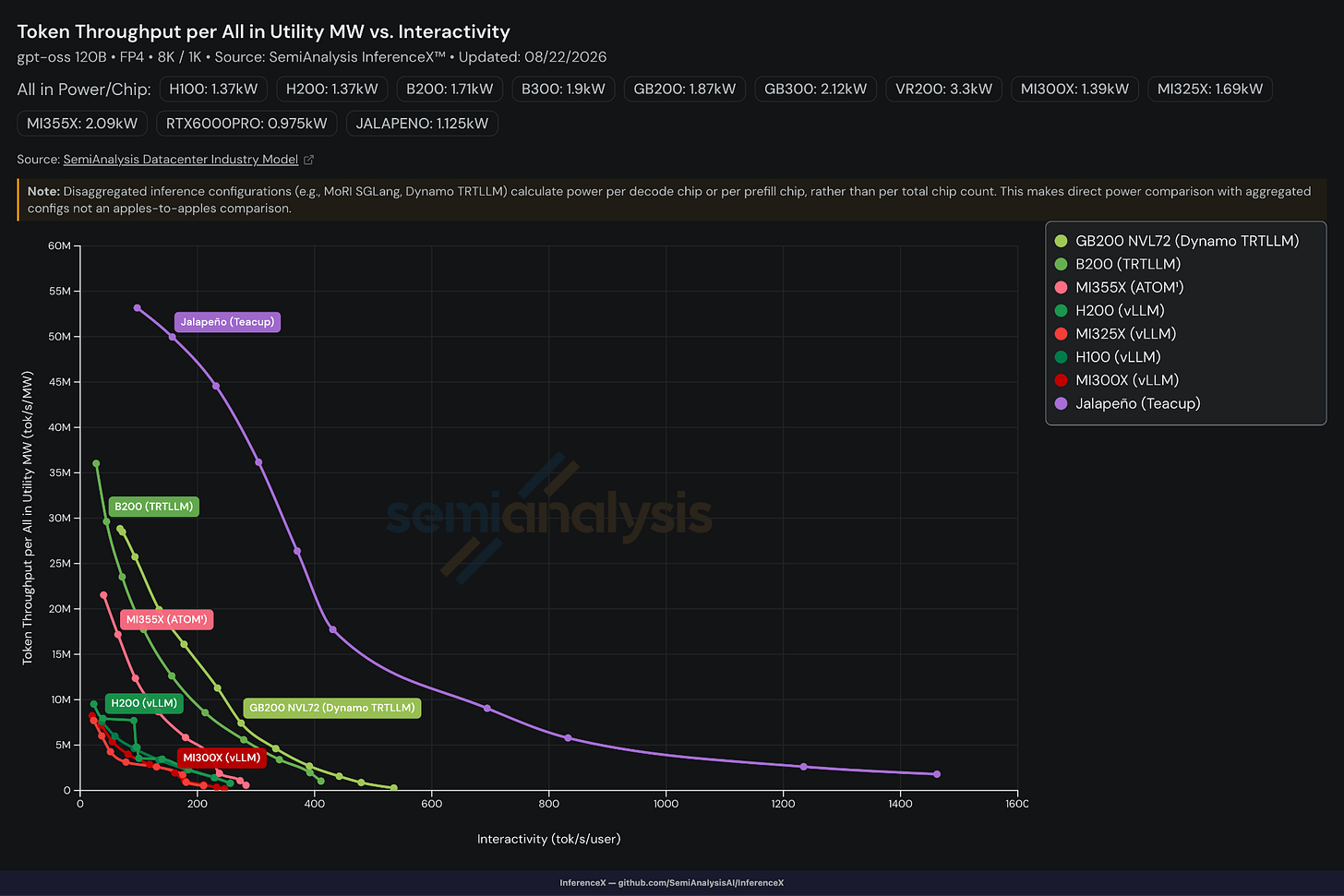
On GPT-OSS, it’s another bloodbath. Jalapeño’s iso-interactivity throughput per MW is nearly double GB200’s highest throughput point and more than 50x GB200’s concurrency 1 point. The higher concurrency Jalapeño points use EP8.
Source: OpenAI, SemiAnalysis
These results are impressive! However, we have to nitpick: they’re just 8k1k, a much easier workload to tune for, and there are no AgentX runs yet. As mentioned in our AgentX article, multiturn, long context workloads stress much more aspects of the serving stack, such as routers and prefix cache. Many more optimizations are needed to excel in agentic workloads. Read more about this in the AgentX article.
Digging into the specs and architecture
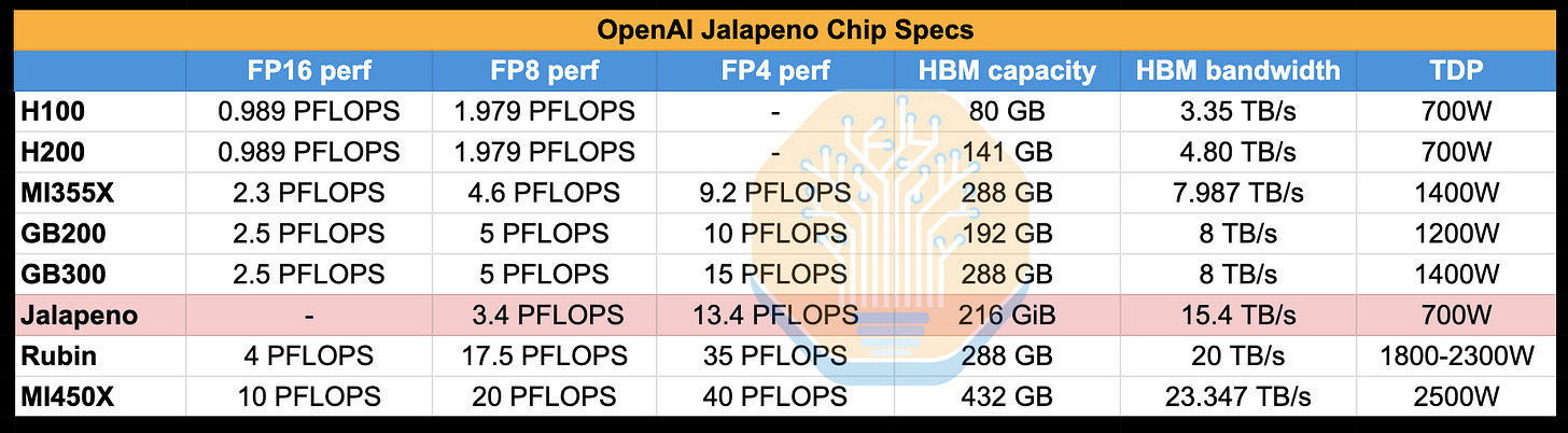
All these results were gathered on the A0 stepping of Jalapeño, just 9 months into the program. But there is already a B0 stepping that is currently in the fab! B0 has optimizations that deliver roughly a 25% perf-per-watt improvement over the earlier A0 silicon. Specifically, the B0 stepping delivers 13.4 PFLOPs of MXFP4 on a single reticle-sized compute die that is manufactured on TSMC’s N3P. This compares to 17.5 PFLOPs of dense Rubin NVFP4 for a single Rubin compute die that is similar size and on the same node.
This is more respectable considering Jalapeño’s TDP is only 700W compared to Rubin’s at 900-1,150W per compute die. As Jalapeño is geared towards inference rather than training, it is understandable that OpenAI doesn’t need to push TDPs higher to maximize FLOPs, but regardless the above shows that Jalapeño delivers respectable peak theoretical FLOPs.
When compared directly to other accelerators, Jalapeño has the highest HBM bandwidth per watt, and the highest FLOPs per watt, comparable to the 1,800W Rubin Max-Q configuration:
Source: SemiAnalysis
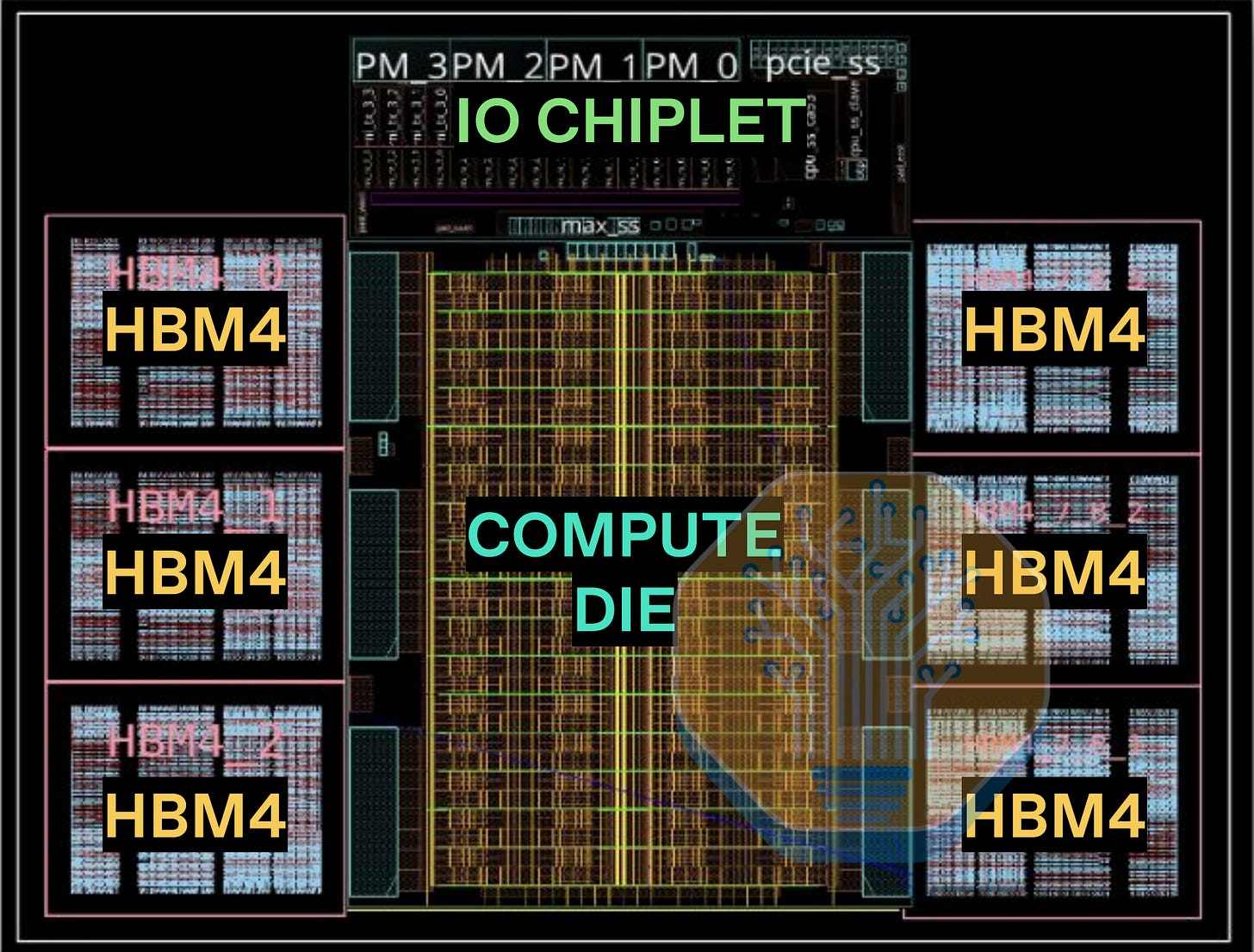
Off-package I/O is provided by an N3E I/O chiplet with 32 lanes of 800G SerDes, for the compute fabric, with 24 lanes (600GB/s) being used for local scale-up within the rack, and 8 lanes (200GB/s) for global scale-up which is the 2,048 XPU multi-rack domain. PCIe Gen 5 is used for system I/O to connect to the x86 host CPU.
Jalapeño will ship with HBM4, making this chip one of the relatively early adopters after Nvidia and AMD, even beating the established TPU and Trainium programs. As one of the key architectural principles behind Jalapeño is getting the most out of HBM bandwidth, settling for anything but the best HBM would run counter to that goal. This results in 15.4TB/s of memory bandwidth per package which bests all the other accelerators shipping that are using HBM3E. The 15.4TB/s bandwidth shows its HBM4 can hit 10Gbps pin speeds, which would give it a slight edge over the 9.6Gbps Nvidia is getting out of its HBM4 in Rubin. The HBM is likely provided by Samsung.
Source: OpenAI
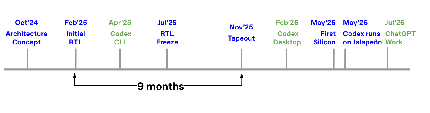
OpenAI taped out Jalapeño in November 2025, or more specifically, this was a tape out of the CoWoS design, not just the top die silicon. Within 9 months of that Nov 2025 tapeout, and with only 3 months of bring-up on actual silicon, OpenAI has already delivered very good results with Jalapeño. This is all the more impressive as the team is starting from zero on the software stack.
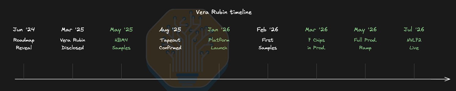
Meanwhile, Rubin’s CoWoS tape out was completed in October 2025, a month earlier, and yet the only early results we have seen are from CoreWeave’s engineering samples. Nvidia has not let us test and release benchmarks in the same way that OpenAI has, indicating their chip software is still immature. The CUDA moat is potentially dead given how fast OpenAI can bring up new models on their silicon.
They are still far from optimized and we can see that generally Jalapeño has delivered better numbers. We don’t think that Nvidia hardware is inferior, but more so that Jalapeño’s software bring-up has progressed more quickly than Nvidia’s. This speaks to the power of hardware/software co-design, which is the main area where a cracked frontier lab ASIC team can excel over more established merchant silicon players. Counterintuitively, starting from scratch may also have benefited OpenAI as it could make clean-sheet architectural decisions without worrying about backwards compatibility or older software versions.
While OpenAI has engineering samples of Jalapeño, production is currently scheduled to gradually ramp over 2027 with most of the output currently scheduled for the end of next year. For more details of unit volumes and ASPs, see the SemiAnalysis Accelerator Model .
Suffice to say, OpenAI Jalapeno is a real high volume ASIC.
When compared against Rubin’s timeline, Jalapeño’s is shockingly quick. As shown earlier, Jalapeño’s results beat Rubin’s despite Rubin’s head start.
Source: SemiAnalysis
Jalapeno Architecture
Digging into the architecture now, the chip’s matrix engine uses MXFP numerical formats and a weight stationary systolic array, similar to TPU. But when compared directly to TPU, it has support for smaller shapes / dimensions, meaning that it doesn’t have weird performance cliffs that get exposed by awkwardly shaped matmuls on bigger systolics.
It also has 64-bit scalar cores and FP32/INT32 vector cores. OpenAI has also invested in redundancy at the tray level and has yield harvesting built in at the core and channel level. They claim that AI assistance in chip design delivered an 8% reduction in SIMD area and a 10% reduction in matrix-engine area during design. While they did not clarify the exact process/voltage/temperature (PVT) conditions, they also mentioned the AI-assisted blocks improved timing and power over the initial blocks.
The Jalapeño architecture design focuses on eliminating memory movement of KVCache and weights as well as fixed latencies and overheads in order to make it possible to get closer to the raw peak flops/bandwidth even for small batches or shapes as compared to other accelerators.
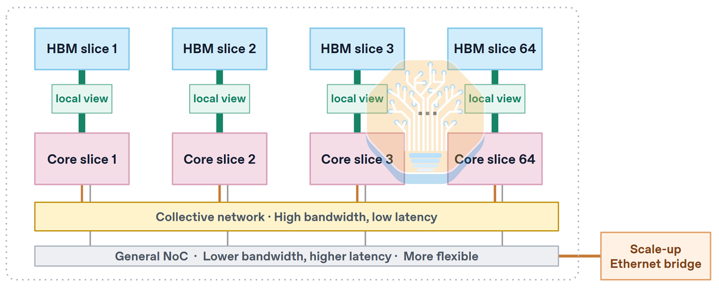
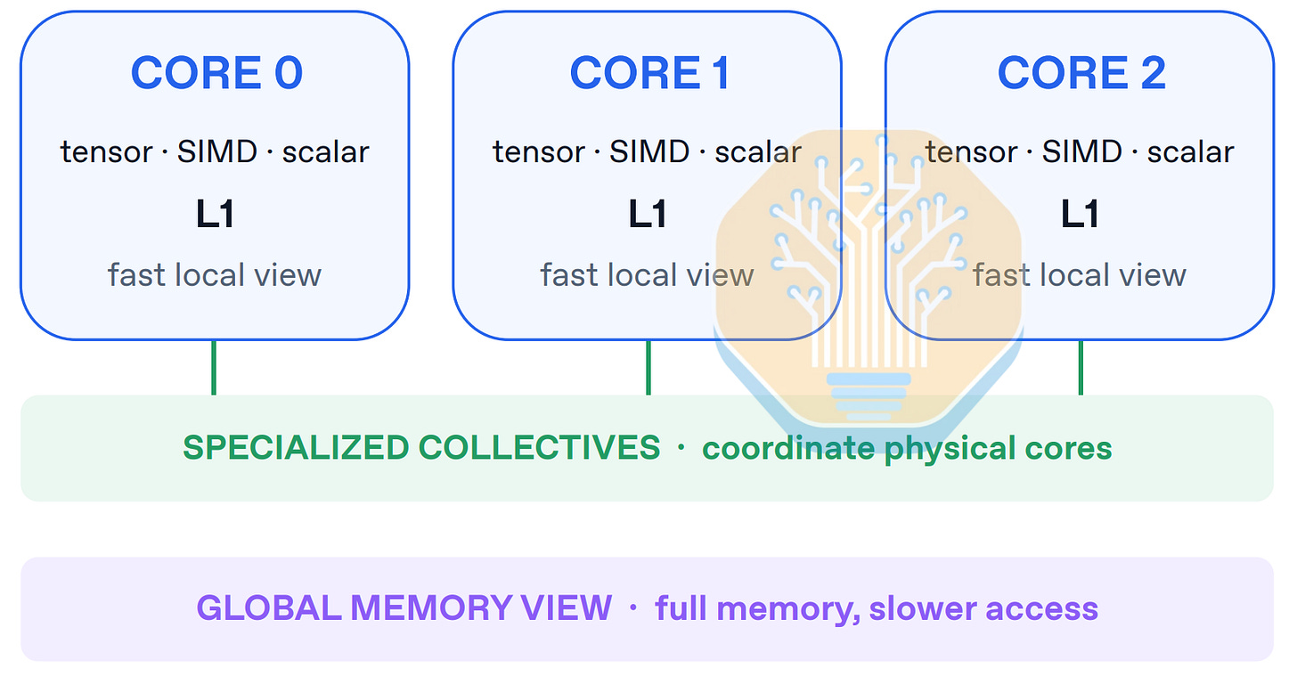
The cores and the HBM are divided into slices, where each core slice has a low-latency local view on its own slice of HBM. Synchronization between slices occurs on a high-bandwidth dedicated collective network. This minimal memory hierarchy already gives Jalapeño a big potential advantage over GPUs, where memory accesses must traverse a complicated memory system, resulting in large latencies that must be amortized or hidden over larger shapes.
This choice is feasible because with careful placement of weights and KVs, synchronization between cores can be restricted to limited, known high-bandwidth comms such as tensor-parallel communication that can be overlapped with compute.
Source: OpenAI
此外还有一个通用 NoC,用于一般通信以及访问扩展(scale-up)网络。总体而言,与 Nvidia 和 Google 相比,OpenAI 通过简化的 NoC 和内存子系统节省了大量功耗,并获得了显著的性能提升。
如果 Jalapeño 取得成功,这将是一个强烈的信号:业界对编程模型以及完美通用编译器的执念,正在被前沿 AI 模型所颠覆。
Software
OpenAI writes Jalapeño kernels like assembly. Each kernel gets hand-tuned code, some running to ~3,000 lines, backed by correctness checks and a custom sanitizer. Early kernel work was human-in-the-loop rather than fully automated, but this shifted with a more scaled-up, internal version of Codex, one which OpenAI plans to pitch to enterprise customers. The internal serving engine is called “Teacup”. Interestingly, OpenAI had no internal implementation of MLA kernels until they benchmarked DeepSeek with InferenceX . The ability for Codex to write functional and efficient kernels so quickly (without any of OpenAI’s kernel engineering team intervening) shows the software pipeline’s developmental ability.
OpenAI programs Jalapeño with Gluon. Gluon is OpenAI’s kernel programming language. Built on top of Triton, Gluon preserves Triton’s SPMD (Single Program Multiple Data) programming model, but it exposes low-level programming abstractions . For example, for NVIDIA GPUs, it offers APIs that map to PTX instructions, including MMA instructions, TMA instructions, mbarrier mechanisms, and many more. The most unique abstraction Gluon provides is the layout . Generally speaking, a layout defines a mapping between a hardware resource (e.g. 5th register of warp 9) and a tensor element (e.g. tensor element on row 6 column 7). Gluon’s layout abstraction is based on Linear Layouts , a type of layout algebra OpenAI invented. Linear Layouts mathematically formalizes what a layout is and provides tools to operate on layouts. This enables many features, such as provably correct layout conversions and optimal memory swizzling.
In terms of Jalapeño’s programming model, each Gluon program maps to a persistent thread. We believe this hints that Jalapeño suits the persistent kernel programming pattern , where each program executes on multiple tiles, and the programmer, rather than the hardware scheduler, assigns the work. OpenAI mentioned TensorInfo, an abstraction that explicitly encodes layouts. This is likely the set of layouts designed for Jalapeño, which will be powered by Linear Layouts. Finally, each core offers data prefetching and decoupled out-of-order units. For example, a user might program a wait on a prefetched data, which is locked behind a semaphore.
In a weird twist of fate, OpenAI models like GPT 5.6 Sol, which currently run on NVIDIA GPUs, have been used to design a chip that poses a real threat to the CUDA moat - NVIDIA’s own GPUs are helping usher in their potential successor in real time.
Comparing across time, we can also see Jalapeño’s developmental pace, achieving more than 2x throughput improvements at certain interactivities in less than 2 weeks. Each tarball we get from the Jalapeño team has a world of wonders inside.
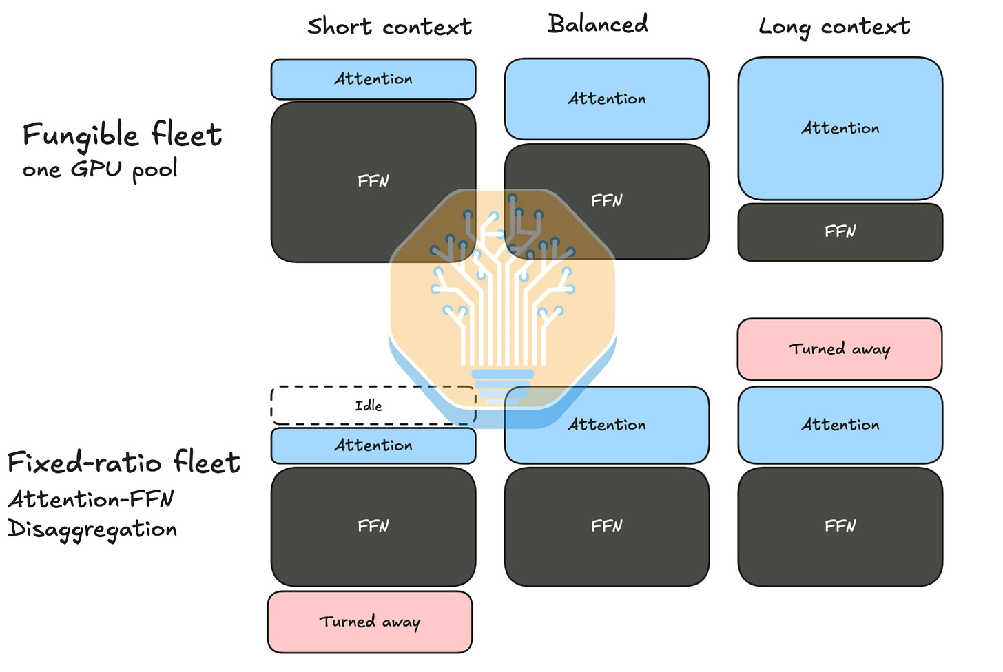
Disaggregation also breaks locality. The prefill worker produces a large KV cache that the decode worker immediately needs, so the system must transfer that state across the network before generation can continue. That adds bandwidth consumption, synchronization, queueing, and another failure domain. The cost also rises with input sequence length because KV cache grows. However, avoiding the movement of KVs is largely a power and latency optimization; being willing to move some KVs around can allow for increased hardware utilization at the expense of some power and per-request latency.
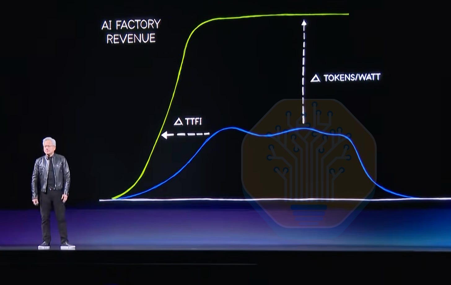
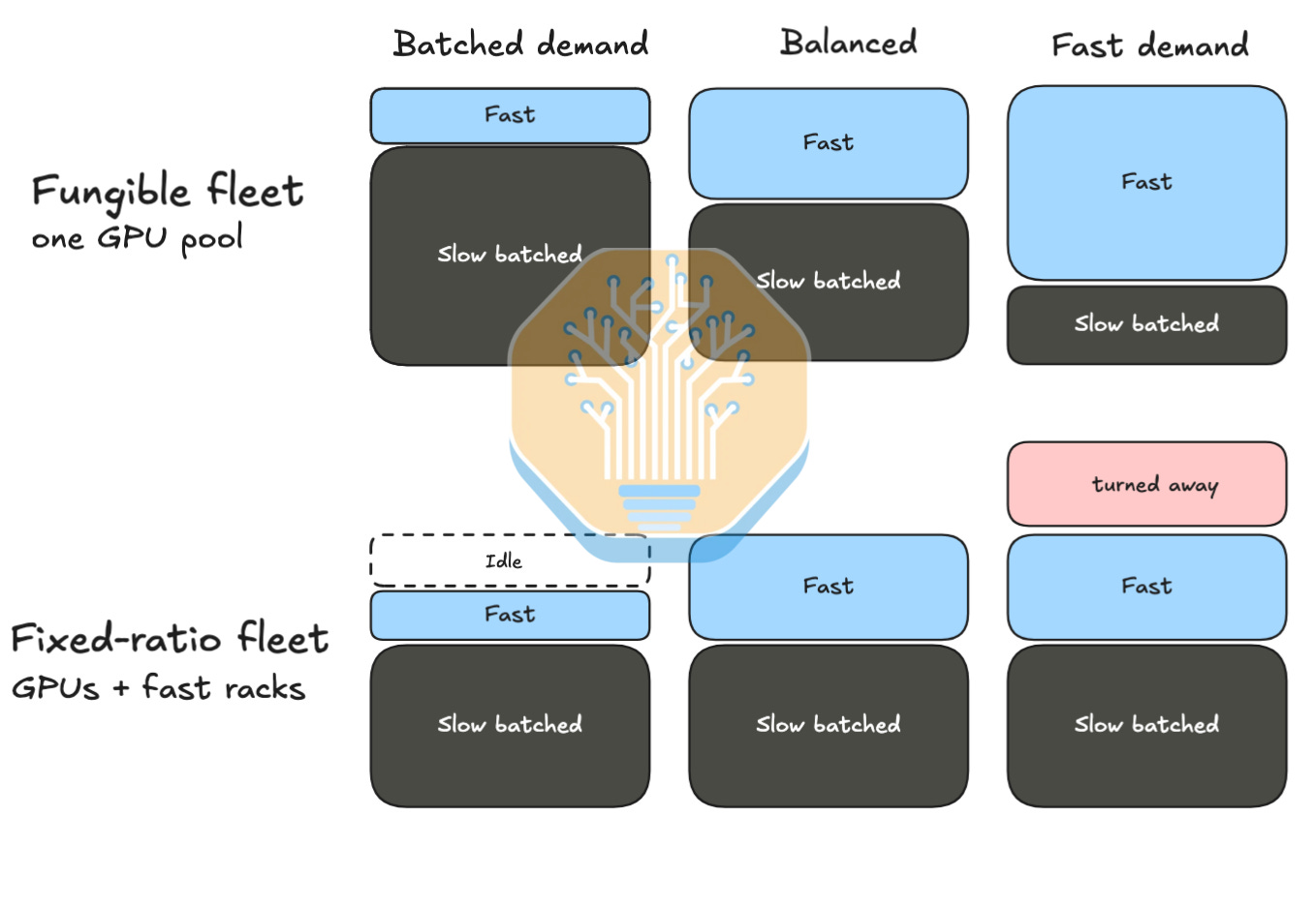
A fungible fleet shifts capacity between latency-sensitive requests and throughput-oriented batches, while a fixed split strands hardware whenever the traffic mix changes. Moreover, context length changes the balance between attention and FFN work, making any fixed hardware ratio efficient only near its design point.
Source: SemiAnalysis
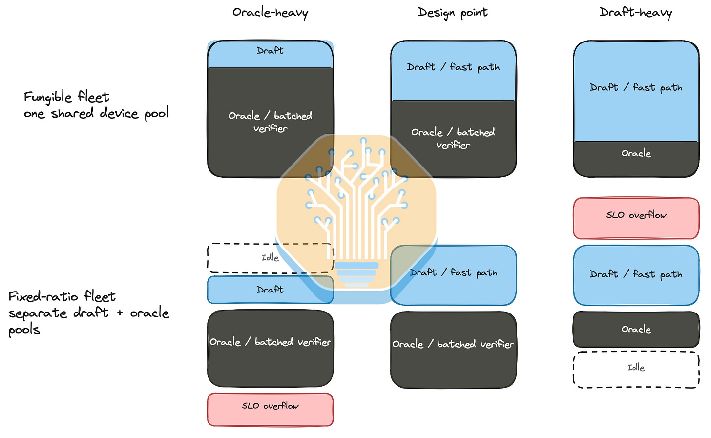
The same constraint applies to speculative decoding. A draft model has to feed candidate tokens to the verifier with extremely low latency. Separating the two across specialized pools turns a tightly coupled decoding loop into a distributed protocol. The extra communication and coordination can consume the latency saved by drafting. Keeping both models on the same devices and low-latency fabric preserves the locality that makes speculation worthwhile in the first place.
Source: SemiAnalysis
However, disaggregation can still win where demand is sufficiently large, stable, and predictable, particularly when conventional GPUs need large phase-specific batches to reach good throughput. But it is not free lunch.
From Japanese to Indian (Mild to Spicy): Katsu, Vindaloo, and Chana - How are the curry dishes put together into a rack system?
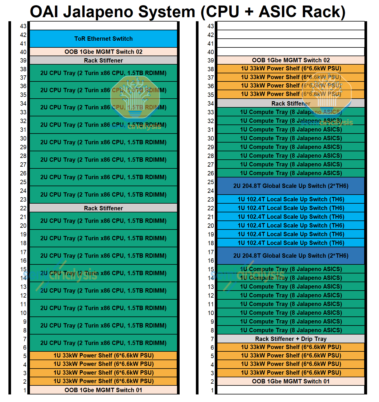
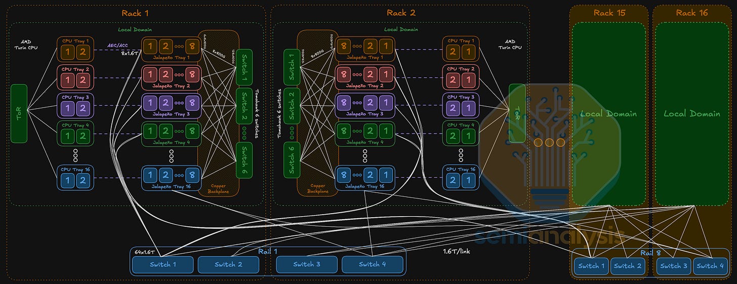
The Jalapeño System at the rack unit level consists of a CPU host rack and an ASIC rack. The host rack houses 16 host CPU trays named “Katsu,” each corresponding to one of the 16 ASIC trays, named “Vindaloo,” to the right of the Katsu. Each host houses two Turin-class AMD EPYC CPUs with 1.5TB of DRAM, 2x E1.S, and 2x M.2 SSDs per rack. Each tray is also specced with 400G (2x200G) frontend networking. Each Katsu tray connects to each Vindaloo tray via 8 external PCIe DAC cables that run horizontally across the rack at the front. The system level design is done in partnership with Celestica.
The ASIC rack consists of 16 Vindaloo trays and 8 scale up switch trays (6 for local + 2 for global), named “Chana.” Each Vindaloo tray consists of 8 Jalapeño ASICs, making up a total of 128 Jalapeño ASICs per rack. The ASICs are connected to each of the Chana switch trays via a copper cable backplane, just like that of Nvidia’s Oberon. The scale up topology is split into a local domain of 128 ASICs within the rack and a global domain connecting up to 16 racks or 2,048 ASICs. We will explain the bandwidth and the topology in more detail below.
Power provisioning to a sidecar host rack draws roughly 50kW provisioned (31kW in production), and the ASIC rack draws 130kW, making the total two rack system roughly 160kW. That’s basically a double-wide GB300 rack in terms of power draw.
Source: SemiAnalysis, OpenAI
OpenAI can connect up to 2,048 Jalapeño XPUs within a single scale-up network. The scale-up network consists of two domains, a local domain connecting all 128 XPUs over backplane within the rack, as well as a global domain connecting 2,048 XPUs over 16 racks using a hybrid of copper and optical interconnect. Each rack consists of 8 Chana switch trays. Six Chana switches in the middle are for the local domain, which come with one 102.4T Tomahawk 6 switch ASIC each. Two Chana switches at the top and bottom of the local switches are for the global domain, which we think could consist of 2x 102.4T Tomahawk 6 switches making up to 204.8T per switch tray.
In the local domain, each of the 128 Jalapeño chips has a per XPU uni-directional bandwidth of 4.8Tb/s and is connected on an all-to-all basis to 6x 102.4Tb/s Tomahawk 6 ASICs. This would amount to 48-differential pair (DP) male and female connector pairs per XPU translating to a total of 6,144DPs worth of passive copper cables per rack used for local scale-up.
For the global domain, 16 racks totaling 2,048 XPUs are connected together via a combination of copper backplane, electrical 204.8T TH6 switch, 1.6T transceivers, and optical circuit switch. Each XPU has a uni-directional bandwidth of 1.6Tb/s for the global link, which is 16-differential pair (DP) male and female connector pairs per XPU for the backplane between the XPU and the global switch. Bandwidth exiting each global switch tray of 2 ASICs each is split between the backplane and front panel optics.
Between local domain and global domain, backplane connector count per rack comes up to 64 DPs per XPU and a total of 8,192 DPs worth of passive copper cables per rack.
The global domain adopts a rail-only architecture consisting of 8-rails across the global domain. We think OpenAI routes optical links in the global domain via Optical Circuit Switches (OCS) installed in every rack. For every XPU, 1.6Tb/s of global bandwidth will travel to the global switch tray over the copper backplane. This then exits the switch through the front panel via 1.6T transceivers, which go to the passive optical switch before exiting the rack. This expands the scale-up world size to 2,048 XPUs combining 16 racks of 128 XPUs each.
Source: SemiAnalysis
Because scale-up networking is only about 10% of total system cost, that flexibility buys valuable optionality for future 10–20 trillion parameter models or 2–4 million token context windows. On deployment, OpenAI is partnering with neoclouds and is gathering reliability data with datacenter partners through January while optimizing dock-to-rack rollout time.
What’s Next
Next, we talk about the future of Jalapeño, whose first production token is coming soon. The next goal is 100MW, and the hurdles will mostly be hardware: How much can they produce, how well can they deploy and operate datacenters, how do they handle monitoring, and resiliency, etc. The software is already proven, and with internal models, every software headstart is easily caught up to. Behind the paywall we will discuss implications for NVIDIA, AMD, Cerebras, and other chip companies who have signed deals with OpenAI in the coming years.
We also cover production volumes, units, and timelines for the next generation chip in our Accelerator model here .